
Testing and Inspection Services for Quality and Performance at Every Stage
At Adonai Technologies, our testing and inspection services guarantee that every product meets the highest standards of quality, functionality, and reliability. By combining advanced inspection techniques with rigorous testing protocols, we help you identify and resolve issues early, ensuring your PCBs and assemblies are ready for real-world applications. Our thorough approach includes functional testing, Automated Optical Inspection (AOI), and X-ray inspection, allowing us to assess each component’s durability and performance under various conditions.
Whether for prototypes or high-volume production, our testing and inspection services are tailored to meet your project’s exact specifications and industry standards. Explore the tabs below to see how our testing and inspection capabilities can ensure the quality of your electronics.
Explore Our Testing and Inspection Services
Functional Testing
Our functional testing service verifies that each assembly performs as expected under real-world conditions. We assess the functionality of circuits, components, and connections, ensuring they meet your specifications and operate reliably within their intended applications.
Key Benefits:
- Verifies operational functionality of every component and connection.
- Detects performance issues early, ensuring reliable performance.
- Essential for mission-critical applications across medical, industrial, and consumer electronics.
Automated Optical Inspection (AOI)
Our Automated Optical Inspection (AOI) uses advanced imaging technology to detect surface defects, component misalignments, and soldering inconsistencies with precision. This fast, accurate inspection method ensures the quality of each PCB assembly, even at high volumes.
Key Benefits:
- Detects solder defects, misalignments, and surface flaws.
- Enables fast, efficient quality control in high-volume production.
- Ensures consistent quality for visually inspectable elements.
X-ray Inspection
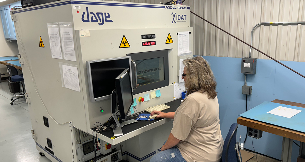
X-ray inspection provides in-depth, non-destructive testing for solder joints and hidden components, enabling us to detect internal defects that are invisible to standard inspections. This technique is especially useful for complex assemblies with Ball Grid Arrays (BGAs) and other components with concealed connections.
Key Benefits:
- Reveals internal defects like solder voids and bridging.
- Essential for high-density boards and Ball Grid Array (BGA) components.
- Provides a non-destructive view of internal connections for quality assurance.
End-of-Line (EOL) Testing and Final Quality Checks
Our End-of-Line (EOL) Testing serves as a final quality check, ensuring each product meets performance and quality standards before shipping. This last step minimizes risks of post-deployment issues and assures clients that every assembly is deployment-ready.
Key Benefits:
- Confirms quality and functionality at the final stage.
- Reduces the risk of field failures post-deployment.
- Ensures consistent quality in high-volume production
